Main page
Tutorial:
FDTD & GPU
Yee's algorithm
Sources
Materials
Boundary conditions
Near-to far field
Application notes
| Application note: Thin film absorption
Calculation of thin film reflection, transmission or absorption can be done analytically
using Fresnel coefficients and related equations. This approach can be used perfectly also for multilayers
and use of FDTD for such purposes is absolutely pointless. However, it can be used as a simple benchmark
of FDTD performance. Moreover, if we want to address films that are to some extent microstructured or nanostructured,
we cannot use conventional methods anymore and we need to seek for a numerical technique.
In this example we show how to calculate thin film absorption and compare it to analytical values.
|
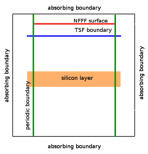
Image on the right shows scheme of the computational volume used for the simulation. As a simplest model, free standing
silicon thin film (1 micrometer) was used for calculation. A normally incident plane wave
was used to enter the selected wavelength into computational volume. No dispersion model was used - for every wavelength we have
used directly the database values for Si_100. Absorption was evaluated locally and averaged in time from the results (using OUT_SUM directive).
Transmitted and reflected intensity was evaluated using point outputs below and above thin film. These intensitites were
normalized to transmitted intensity values calculated using the same model but without the film (this value was treated as incident wave
intensity).
|
 |
|
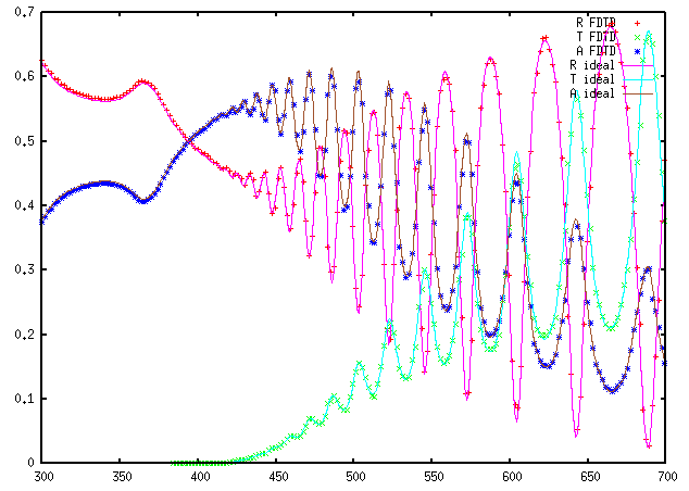
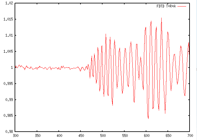
A result of calculation for range of 300-700 nm is shown below, compared to the same quantities obtained using analytical equations. On the left side
the absorption, transmission and reflection spectra are shown. On the right side, their sum is shown to estimate the numerical
errors of the calculation (the ideal value is 1).
|
|
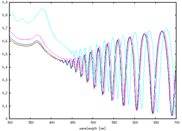
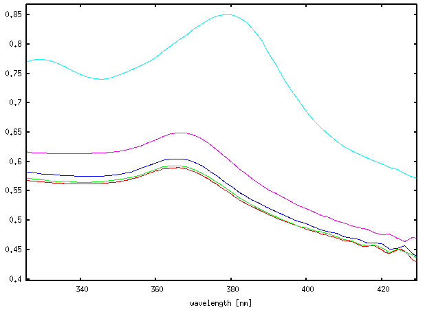
It is important to note that, namely for smaller wavelengths, the result strongly depends on discretisation. In the above case, discretisation of
2.5 nm was used. Even this might be too large for small wavelengths where light penetration depth in silicon is small (which leads to large numerical errors
in absorption summation). If we increase the discretisation even more we can see that this effect is more and more pronounced, as shown on whole spectrum (left)
and detail (right) in the following image. The red curve is analytical value, the other curves are for discretisation of 2.5 nm, 5 nm, 10 nm and 20 nm (larger
is worse).
|
(c) Petr Klapetek, 2013
|